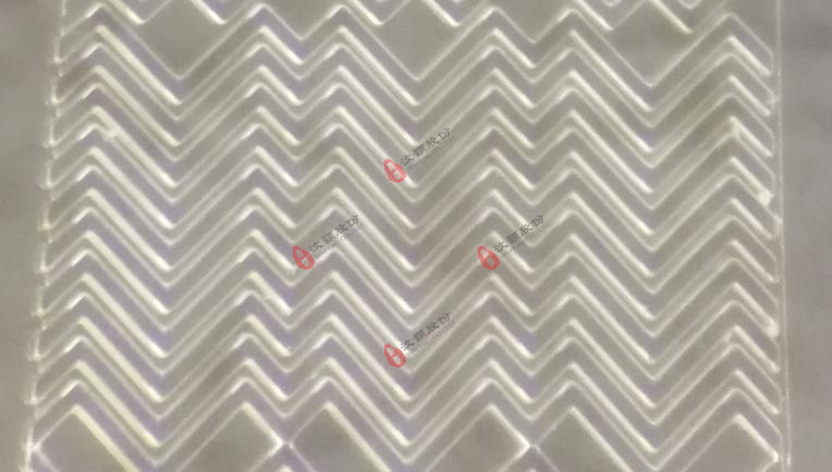
SU-8 Photoresist Mold
1. Su-8 silicon wafer mold introduction:
Mold is often used in the process of microfluidic chip processing, especially in the process of PDMS chip processing. PDMS chip processing is usually made by soft lithography. In order to perform the process of PDMS soft lithography, a template is usually used. The most common and frequently used template must be an epoxy resin su-8 mould.
Brunei hao finds shares using the lithography technology in coating SU - 8 photoresist on preparation of deep wide than high silicon microstructure and micro parts, thickness can be made in 10-500 mu, has certain mechanical strength of the mold, using lithography process pattern, can be used for PDMS casting, experiment is realized by bonding the carrier, a single set of moment can satisfy the deep wide ratio 1:1 ~ now.
Micromould is a kind of special material mould with micron-level pattern structure, which is necessary for the manufacture of microfluidic chip and other biological chips. The micro mould is based on the processing technology of photolithography. According to the differences of the forming process and application range, we provide PDMS mould products.
Micromould product :PDMS mould
Purpose: making PDMS products
Mold outside diameter: standard silicon substrate size 2 inch, 3 inch, 4 inch, 5 inch, 6 inch
Groove depth :40-300
The width of the groove is greater than or equal to 1
Mold thickness :1mm
Short time limit for a project:
2. Examples of su-8 silicon wafer mould products are as follows:

圖 厚度分別為30μ、50μ、200μ、500μ SU-8硅片模具
3. Local structure enlargement
(1) single-layer structure: only one layer of photoresist is applied to the silicon wafer, and the exposure is completed once

圖為:單層SU-8光刻膠模具局部結構放大圖
(2) multilayer structure: the composite structure with laminated layers can be made by coating the silicon wafer with photoresist for many times and exposing for many times

圖為:多層SU-8光刻膠模具局部結構放大圖

PDMS mold:
The terminal su-8 mould is a micro mould directly obtained by using the SU-8 photoresist after photoresist curing.
Both ends are used and affordable.
Ending is suitable for small batch PDMS chip replication.
The su-8 mold processing process can be divided into 9 main steps. According to the order of mold processing, it is shown as follows:
1. Prepare the wafer/wafer
2. Spin coating negative su-8 photoresist
3. Soft baking (the first baking of photoresist)
4. Removal of edge photoresist (optional)
5. Ultraviolet exposure
6. Baking after exposure (the second baking of photoresist)
7, development
8. Hard baking (the third baking of photoresist) (optional)
9. Check
Note: this paper mainly takes silicon wafer as an example. Of course, other substrate such as surface modified glass can also be used.
Common equipment/consumable materials used in epoxy resin su-8 mould processing: plasma processor, homogenizer (rotary coating machine), uv exposure machine, hot plate, su-8 developer, etc.
